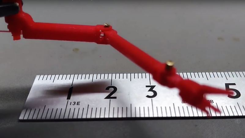
Homemade semiconductors sound like the sort of hobby that begins with “I watched one video” and ends with a garage that looks suspiciously like a moon base. Yet the idea is not science fiction. Hobbyists, engineers, and relentlessly curious makers have shown that small-scale chipmaking can be explored outside billion-dollar fabs, as long as expectations stay realistic and safety stays in the driver’s seat. One of the most interesting tools in that world is not a giant lithography machine or a room-sized furnace. It is a tiny vacuum chamber arm.
A tiny vacuum chamber arm may look almost comically small, but its job is serious. In homemade semiconductor work, a vacuum chamber is often used for thin-film deposition, sputtering, plasma experiments, sample handling, and other processes where air is the enemy. Once the chamber is sealed and pumped down, however, the experiment becomes a ship in a bottle. You can see the workpiece, but you cannot simply reach in and nudge it. That is where a compact manipulator arm becomes useful: it gives the builder a way to move a wafer, sample, mask, or small fixture inside a sealed environment without ruining the vacuum.
The concept became especially fascinating in the DIY electronics community because it takes a very professional semiconductor problem and shrinks it into a maker-scale challenge. Commercial fabs use precise robotic handlers, vacuum transfer systems, cleanroom-compatible components, and expensive process tools. A home lab cannot copy that entire infrastructure, but it can borrow the underlying idea: control motion, reduce contamination, and keep the process environment stable. In plain English, the tiny arm is the lab assistant that fits in the jar.
Why a Vacuum Chamber Matters in Homemade Semiconductors
Semiconductor fabrication is built on controlled layers. A typical device starts with a substrate, often silicon, then gains or loses material through repeated steps such as cleaning, oxidation, patterning, deposition, etching, and heat treatment. Even simple homemade devices require discipline because tiny flaws can create very large problems. Dust, fingerprints, moisture, and uneven films are the villains of this story, and they do not even have the decency to wear capes.
Vacuum processing helps because many thin-film techniques work better when unwanted gases are removed. In physical vapor deposition, for example, a material can be vaporized or sputtered so that it travels through a low-pressure chamber and lands on a target surface as a thin layer. This can create metal contacts, conductive films, or experimental coatings. In plasma-based processes, low pressure helps maintain the plasma conditions needed for etching or surface treatment. The vacuum chamber is not just a box; it is a controlled stage where the physics can behave more predictably.
For homemade semiconductors, the chamber also becomes a proving ground. Before anyone dreams of complex integrated circuits, they usually need to master smaller victories: creating a clean film, coating a small piece of silicon, aligning a sample, or repeating a result without turning the entire project into a mystery novel. A tiny vacuum chamber arm supports those goals by letting the builder reposition samples without opening the chamber every few minutes.
What the Tiny Vacuum Chamber Arm Actually Does
A vacuum chamber arm is a miniature manipulator designed to move objects inside an evacuated chamber. In a simple setup, it may only push, pull, rotate, or lift a sample holder. In a more ambitious design, it can behave like a small articulated arm with multiple segments. The clever part is not only the arm itself, but how it is controlled from outside the chamber.
The DIY design that inspired this topic used an idea similar to surgical tools and compact robotic linkages: slim segments controlled by cables. Instead of running control cables directly through the chamber wall and creating more leak points, the motion can be transferred using magnets through glass or another non-magnetic barrier. That is the key trick. Magnetic coupling allows an external control movement to influence an internal mechanism while the chamber remains sealed.
This is the same general principle behind many professional vacuum motion systems. Commercial sample manipulators and transfer arms often rely on either vacuum-tight mechanical feedthroughs or magnetic coupling. A magnetic design is attractive because it can keep the vacuum boundary intact. The outside handle, knob, or driver moves in normal air; the inside part follows along inside the chamber. No dramatic hiss, no ruined pump-down, and ideally no tiny leak that makes the vacuum gauge laugh at you.
Magnetic Coupling: The Elegant Shortcut
Magnetic coupling is one of those engineering ideas that feels obvious only after someone else has made it work. Place magnets outside a chamber wall, place magnetic or magnet-coupled parts inside, and motion can be transmitted without a physical shaft piercing the wall. For a tiny vacuum chamber arm, this can mean fewer seals, fewer contamination paths, and a simpler way to experiment with motion.
However, elegant does not mean effortless. Magnetic coupling has limits. The chamber wall thickness matters. The distance between the magnets matters. The weight of the internal arm matters. Friction, backlash, and misalignment all matter. If the arm is too heavy or sticky, the external magnets may move while the inside arm politely refuses to cooperate. At that point, the device becomes less of a manipulator and more of a tiny sculpture with trust issues.
Materials also matter. Vacuum environments punish casual material choices. Some plastics can outgas, meaning they release trapped vapors under vacuum. Lubricants can contaminate surfaces. Metals may seize or gall if used carelessly. In professional systems, stainless steel, ceramics, dry lubricants, special polymers, and carefully selected greases are common for good reasons. A home design does not need to imitate a national lab perfectly, but it does need to respect the same principles.
The Role of Thin-Film Deposition
Thin-film deposition is one of the main reasons a homemade semiconductor builder might want a vacuum chamber in the first place. A semiconductor device needs controlled layers: conductors for contacts, insulators for separation, and sometimes semiconductor or dopant-related films depending on the project. These layers may be only a tiny fraction of the thickness of a human hair, yet they determine whether the final device behaves like an electronic component or a shiny disappointment.
In a hobby-scale lab, thin-film deposition might be used to create metal contacts on silicon, coat test pieces, or explore how different materials affect conductivity. The tiny arm can help by moving a sample into position, flipping a small holder, changing exposure angle, or placing a shutter between a source and a wafer. Even basic movement can improve repeatability because the builder does not need to vent the chamber, handle the sample, reseal everything, and pump down again after every adjustment.
Repeatability is the quiet hero of semiconductor work. Anyone can sometimes get one interesting result. The harder challenge is getting the result again, then again, then again after lunch when the room is warmer and the coffee has worn off. A small internal arm helps make the process less dependent on luck and finger gymnastics.
Homemade Semiconductors Are About Systems, Not Just Chips
When people hear “homemade semiconductor,” they often imagine a finished computer chip popping out of a garage like a loaf of bread. Reality is much more layered. A home semiconductor project is really a collection of systems: a clean workspace, controlled heating, patterning, photoresist handling, etching, deposition, measurement, documentation, and safety planning. The chip is the headline, but the toolchain is the story.
That is why a tiny vacuum chamber arm is so compelling. It is not a chip by itself. It is a tool that makes other tools more useful. A spin coater may help apply a resist film. A hot plate may help bake coatings. A furnace may support thermal processing. A vacuum chamber may enable deposition. A microscope may help inspect patterns. The manipulator arm connects to this ecosystem by improving sample handling inside the vacuum step.
For educational labs and advanced hobbyists, this kind of tool also teaches the right mindset. Semiconductor fabrication is not magic. It is controlled contamination avoidance, controlled geometry, controlled chemistry, controlled heat, and controlled patience. The more controlled the process becomes, the less the builder has to rely on “maybe it worked because Jupiter was aligned with my pressure gauge.”
What Makes the Tiny Arm Hard to Build Well
1. Vacuum Compatibility
Parts that behave nicely on a workbench may behave badly under vacuum. Materials can release vapor, adhesives can weaken, and lubricants can migrate. A tiny arm must use materials that do not contaminate the chamber or the sample. This is especially important during deposition, where stray contamination can become part of the film.
2. Mechanical Precision
A manipulator does not need to be perfect, but it must be predictable. If the external control moves one way and the internal arm responds with a shrug, the tool is not useful. Cable-driven segments, small joints, and magnetic couplings all introduce flex and delay. The design challenge is to make motion smooth enough for real sample handling.
3. Chamber Space
Small vacuum chambers are crowded. The arm must fit around sample holders, electrodes, deposition sources, viewports, wiring, and fixtures. A compact design is valuable because every millimeter inside the chamber has a job. It is basically New York real estate, but with plasma.
4. Cleanliness
Semiconductors dislike dirt with a passion. Any moving part can create particles through friction or wear. That means the arm should be designed to minimize scraping, shedding, and unnecessary contact. The cleaner the motion, the better the chance of getting useful results.
5. Safety
Vacuum systems, high temperatures, high voltage, plasma, glass vessels, and corrosive processing materials can be hazardous. A serious project needs proper shielding, ventilation, training, supervision where appropriate, and a strong habit of stopping when conditions are uncertain. Curiosity is wonderful; preventable accidents are not part of the syllabus.
Why This Tiny Tool Feels So Futuristic
The tiny vacuum chamber arm feels futuristic because it compresses several high-end engineering ideas into a small, visible object. It blends robotics, vacuum technology, materials science, semiconductor processing, and old-fashioned maker cleverness. It is also satisfying because the problem is easy to understand: the thing is inside the sealed chamber, and your hand is outside. Now what?
That simple problem leads to deep engineering. How do you move through a barrier without breaking the barrier? How do you grip a sample without contaminating it? How do you make a part small enough to fit inside a chamber but strong enough to be useful? How do you test it before trusting it near a fragile wafer? Those questions are exactly the kinds of questions that turn a hobby project into real engineering education.
There is also a philosophical appeal. Modern semiconductor manufacturing is famously expensive and complex. The biggest fabs cost enormous sums and rely on global supply chains, ultra-clean environments, and thousands of specialized components. A homemade vacuum chamber arm does not compete with that world. Instead, it makes the world less mysterious. It says: here is one tiny piece of the puzzle, and you can understand it.
What DIY Chipmakers Can Learn From the Project
The first lesson is that toolmaking comes before chipmaking. Many beginners want to jump directly to the finished device, but semiconductor work rewards infrastructure. Better handling, cleaner samples, better logs, improved fixtures, and repeatable motion can matter as much as the glamorous process step everyone talks about online.
The second lesson is that small improvements compound. A better sample holder reduces handling errors. A better chamber arm reduces venting cycles. Better alignment improves film coverage. Better documentation makes troubleshooting possible. None of these improvements feels heroic alone, but together they move a project from “interesting chaos” toward actual fabrication.
The third lesson is that DIY does not mean careless. The best home-lab semiconductor projects are not reckless shortcuts. They are careful adaptations. They take inspiration from professional systems while scaling down the goal. A homemade lab might aim for simple diodes, transistors, test structures, sensors, or educational demonstrations rather than modern processors. That is still impressive. Nobody needs to build a cutting-edge GPU in a garage to learn something profound about how electronics are made.
The Bigger Picture: Garage Fabs, Education, and Accessible Hardware
Interest in homemade semiconductors has grown because chips have become central to almost everything: phones, cars, medical devices, appliances, cameras, industrial controls, and the servers that keep our digital lives humming. At the same time, the manufacturing process is hidden from most people. We can buy a microcontroller for a few dollars, but the journey from sand-like raw material to patterned silicon still feels like a locked room.
Small tools like a tiny vacuum chamber arm help unlock that room, at least conceptually. They show that semiconductor fabrication is made of understandable steps. Difficult steps, yes. Expensive steps at scale, absolutely. But still steps. A student who sees a sample move inside a vacuum chamber can connect the physical motion to deposition, alignment, and process control. That is a much richer lesson than simply memorizing that chips are made in cleanrooms.
This matters because accessible hardware often inspires new builders. The early personal computer movement did not replace mainframes overnight; it gave curious people a way to touch the technology. DIY semiconductor tools may play a similar educational role. They can demystify fabrication, inspire better open hardware, and encourage practical learning in materials science and electronics.
Practical Experience: Lessons From Working Around a Tiny Vacuum Chamber Arm
The most valuable experience with a tiny vacuum chamber arm is learning that motion inside a chamber should be boring. That may sound disappointing, but boring is beautiful in a lab. If the arm moves smoothly, stops where expected, does not scrape, does not shed particles, and does not force the chamber to be opened unnecessarily, it is doing its job. The drama should stay in the science, not in the sample holder falling off at the worst possible moment.
A smart workflow begins outside the chamber. Before trusting any tiny manipulator near a delicate sample, it should be tested in normal air with harmless blanks. This reveals whether the joints bind, whether the magnetic coupling slips, whether the cable path is too loose, and whether the grip is awkward. Many failures are easier to fix on the bench than after the chamber is sealed. In practice, this means the best builders spend more time rehearsing than improvising.
Another hard-earned lesson is that visibility changes everything. A movement that seems easy on the bench may become awkward when viewed through a curved glass wall or a small viewport. Depth perception can be strange. Reflections can hide the exact position of the gripper. Lighting can make a shiny sample look like it is in one place when it is actually a few millimeters away. Good chamber lighting and simple visual reference marks can make the arm feel far more controllable.
Patience also becomes a tool. Vacuum work has a rhythm: prepare, inspect, seal, pump down, wait, observe, adjust, log, and only then make the next decision. Rushing usually creates extra work. A tiny arm encourages patience because it gives the operator a way to make small adjustments instead of constantly restarting the process. That can save time, but more importantly, it protects the sample from repeated handling.
Clean habits matter as much as clever mechanisms. Every part that goes into the chamber should be treated as a potential source of contamination. The arm should not be touched casually, stored uncovered, or modified with mystery materials that seemed fine in a desk drawer. Semiconductor work rewards boring cleanliness: covered parts, labeled samples, careful inspection, and notes that explain what changed between runs.
Documentation may be the least glamorous experience, but it is one of the most important. Record what sample was used, how it was positioned, what movement was made, what the chamber conditions were, and what the result looked like afterward. Without notes, every successful film becomes folklore. With notes, even a failed run becomes useful data.
Finally, the tiny vacuum chamber arm teaches humility. It shows that semiconductor fabrication is not one heroic trick. It is a chain of small disciplines. A clean fixture, a stable vacuum, a predictable motion, a good film, a careful inspection, and a repeatable result all depend on each other. When the arm finally moves a sample exactly as intended, it may not look dramatic. But in homemade semiconductor work, that quiet little movement can feel like opening a door to an entire hidden industry.
Conclusion
A tiny vacuum chamber arm to help with homemade semiconductors is more than a clever gadget. It is a symbol of what happens when maker culture meets serious process engineering. By enabling movement inside a sealed chamber, the arm supports thin-film deposition, sample positioning, cleaner workflows, and better repeatability. It also reminds us that semiconductor fabrication is not only about the final chip; it is about the tools, habits, and careful thinking that make the chip possible.
No tiny manipulator will turn a garage into a modern commercial fab overnight, and that is not the point. The point is learning. The tiny vacuum chamber arm makes a difficult process more visible, more interactive, and more approachable. For builders exploring DIY semiconductor fabrication, it is a small tool with a big lesson: when you can control the environment and the motion, you are one step closer to controlling the result.